(A)The composition principle of the switching power supply
1.1 Input circuit
Linear filter circuit, surge current suppression circuit, rectifier circuit.
Function: Convert the input grid AC power supply into the DC input power supply of the switching power supply that meets the requirements.
1.1.1 Linear filter circuit
Suppress harmonics and noise
1.1.2 Surge filter circuit
Suppress surge current from the grid
1.1.3 Rectifier circuit
Convert AC to DC
There are two types: capacitor input type and choke coil input type. Most switching power supplies are the former
1.2 Conversion circuit
Contains switching circuit, output isolation (converter) circuit, etc. It is the main channel for switching power supply conversion, and completes the chopping modulation and output of the power supply waveform with power.
The switching power tube at this level is its core device.
1.2.1 Switching circuit
Drive mode: self-excited, externally excited
Conversion circuit: isolated, non-isolated, resonant
Power devices: The most commonly used are GTR, MOSFET, IGBT
Modulation mode: PWM, PFM, and hybrid. PWM is the most commonly used.
1.2.2 Converter output
Divided into shaft-free and shaft-with. No shaft is required for half-wave rectification and current-doubler rectification. Shaft is required for full-wave.
1.3 Control circuit
Provide modulated rectangular pulses to the drive circuit to adjust the output voltage.
Reference circuit: Provide voltage reference. Such as parallel reference LM358, AD589, series reference AD581, REF192, etc.
Sampling circuit: Take all or part of the output voltage.
Comparison amplification: Compare the sampling signal with the reference signal to generate an error signal for controlling the power supply PM circuit.
V/F conversion: Convert the error voltage signal into a frequency signal.
Oscillator: Generate high-frequency oscillation wave
Base drive circuit: Convert the modulated oscillation signal into a suitable control signal to drive the base of the switch tube.
1.4 Output circuit
Rectification and filtering
Rectify the output voltage into pulsating DC and smooth it into a low-ripple DC voltage. Output rectification technology now has half-wave, full-wave, constant power, current doubling, synchronous and other rectification methods.
(B) Analysis of various topological power supplies
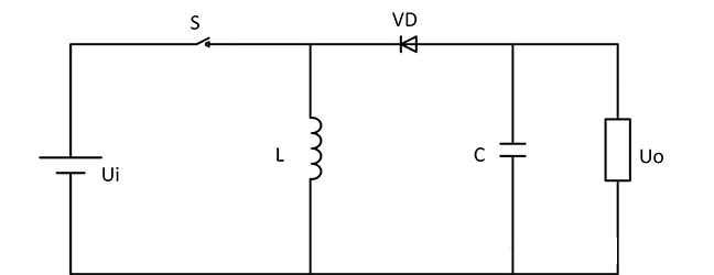
2.1 Buck converter
Buck circuit: Buck chopper, input and output polarity are the same.
Since the volt-second product of inductor charge and discharge is equal in steady state, input voltage Ui, output voltage Uo; therefore:
(Ui-Uo)ton=Uotoff
Uiton-Uoton=Uo*toff
Ui*ton=Uo(ton+toff)
Uo/Ui=ton/(ton+toff)=▲
That is, the input and output voltage relationship is:
Uo/Ui=▲ (duty cycle)
Buck circuit topology
When the switch is turned on, the input power is filtered by the L inductor and the C capacitor to provide current to the load end; when the switch is turned off, the L inductor continues to flow through the diode to keep the load current continuous. The output voltage will not exceed the input power voltage due to the duty cycle.
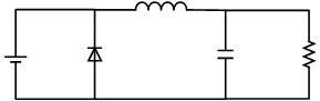
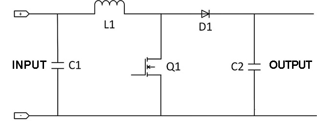
2.2 Boost Converter
Boost circuit: boost chopper, input and output polarity are the same.
Using the same method, according to the principle that the charging and discharging volt-second product of the inductor L is equal in steady state, the voltage relationship can be derived: Uo/Ui=1/(1-▲)
 Boost circuit topology
The switch tube Q1 and the load of this circuit are connected in parallel. When the switch tube is turned on, the current passes through the inductor L1 to smooth the wave, and the power supply charges the inductor L1. When the switch tube is turned off, the inductor L discharges to the load and the power supply, and the output voltage will be the input voltage Ui+UL, so it has a boost effect.
2.3 Flyback Converter
Buck-Boost Circuit: Boost/Buck Chopper, input and output polarity are opposite, and the inductor is transmitted.
Voltage relationship: Uo/Ui=-▲/(1-▲)
Buck-Boost Circuit Topology
When S is on, the load power supply only charges the inductor. When S is off, the power supply is discharged to the load through the inductor to achieve power transmission.
Therefore, the L inductor here is a device for transmitting energy.
(C) Application fields
The switching power supply circuit has the advantages of high efficiency, small size, light weight, and stable output voltage, so it is widely used in communications, computers, industrial automation, household appliances and other fields. For example, in the computer field, the switching power supply has become the mainstream of computer power supply, which can ensure the stable operation of computer equipment; in the field of new energy, the switching power supply is also playing an important role as a device that can stably convert energy.
In short, the switching power supply circuit is an efficient and reliable power conversion circuit. Its working principle is mainly to convert the input electrical energy into a stable and reliable DC power output through high-frequency switching conversion and rectification filtering.
Post time: Oct-10-2024